1. Quantum transport in graphene and carbon
nanostructures
Carbon nanotubes and graphene (Nobel Prize 2010) are
revolutionising the study of semiconductors and offer
the potential for a new generation of devices which may
supplant silicon. This project aims to study the
electrical properties of graphene and carbon
nanostructures in high magnetic fields where the
electrical conduction is strongly influenced by quantum
effects giving rise to phenomena such the Quantum Hall
Effect and Coulomb Blockade. By studying nanostructures
which are typically only a few nanometers in size the
energy levels and transport can be controlled and
modified to create new properties and behaviour.
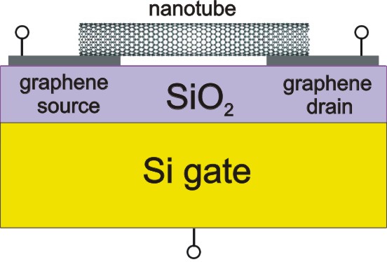
The structures to be studied will be made using a
recently installed next generation electron beam
lithography system capable of writing features down to a
size of 20nm and it is planned to experiment with
combining these with carbon nanotubes also.
2. Carbon based PhotoVoltaic Devices
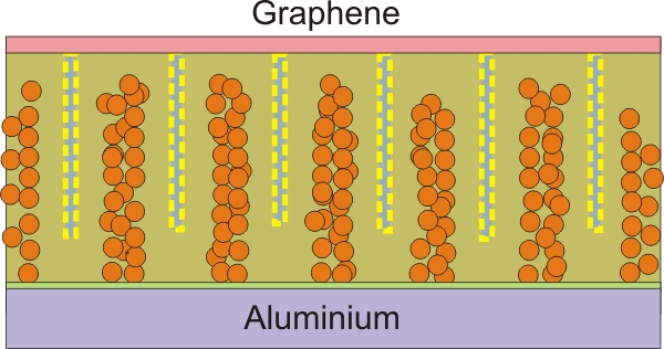 Finding new ways to produce Photovoltaic
(PV) cells with high efficiencies and novel
manufacturing techniques is a challenge for
semiconductor physics. This project will explore the use
of graphite, carbon nanotubes and polymer semiconductors
to produce new structures which can act as PV devices
with responses in both the visible and infrared part of
the spectrum. The project will combine optical
spectroscopy of carbon nanotube/polymer nanostructures
with studies of electrical properties and fabrication
techniques. Finding new ways to produce Photovoltaic
(PV) cells with high efficiencies and novel
manufacturing techniques is a challenge for
semiconductor physics. This project will explore the use
of graphite, carbon nanotubes and polymer semiconductors
to produce new structures which can act as PV devices
with responses in both the visible and infrared part of
the spectrum. The project will combine optical
spectroscopy of carbon nanotube/polymer nanostructures
with studies of electrical properties and fabrication
techniques.
The experiments will use techniques such as
PhotoLuminescence Excitation (PLE) spectroscopy to study
the transfer of energy and charge through different
components of the cells and infrared spectroscopy to
examine the behaviour of transparent conducting layers
such as graphene and nanotubes. These techniques will be
combined with electroluminescence and photoresponse to
evaluate the potential efficiency of the devices.
|
